


 You're on the Project VGA Page


Communication
Update 2007/11/15: Added block diagramPosted on 2007/10/31 - 01:26
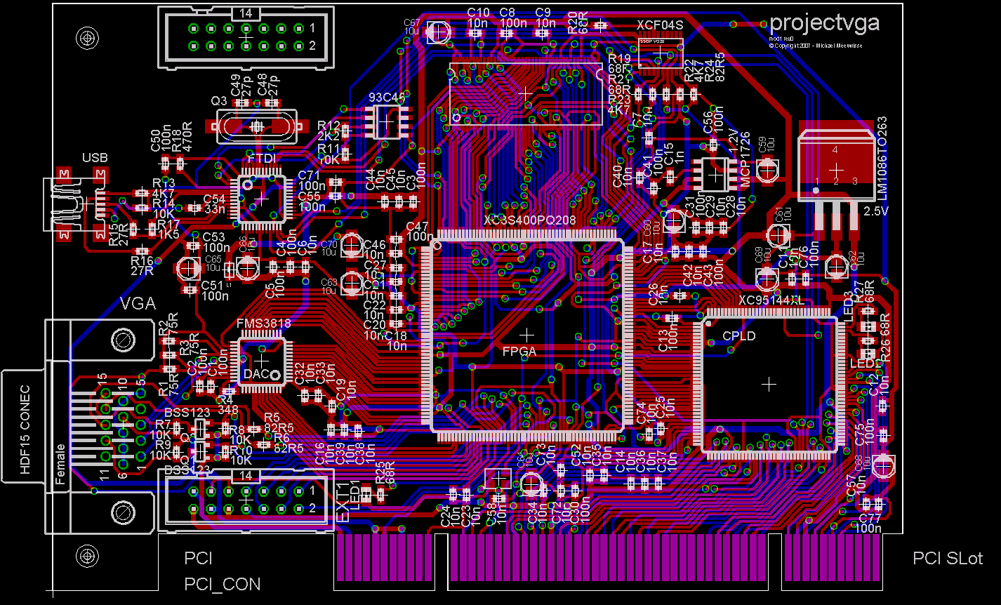
As predicted I didn't do anything on the project last week and probably won't do anything this week either. All the other classes have a priority right now since the deadlines are 2nd (for one class) and 8th (for the other) of November. Fun. I also forgot to mention the updated schematic last time, get it here, or see the image below if you don't have Eagle. I've got two little issues remaining, one being that I don't know if I'll pull up or pull down HSWAP_EN (bank 0) of the FPGA, and pull up, down or float PWREN# of the FT2232.
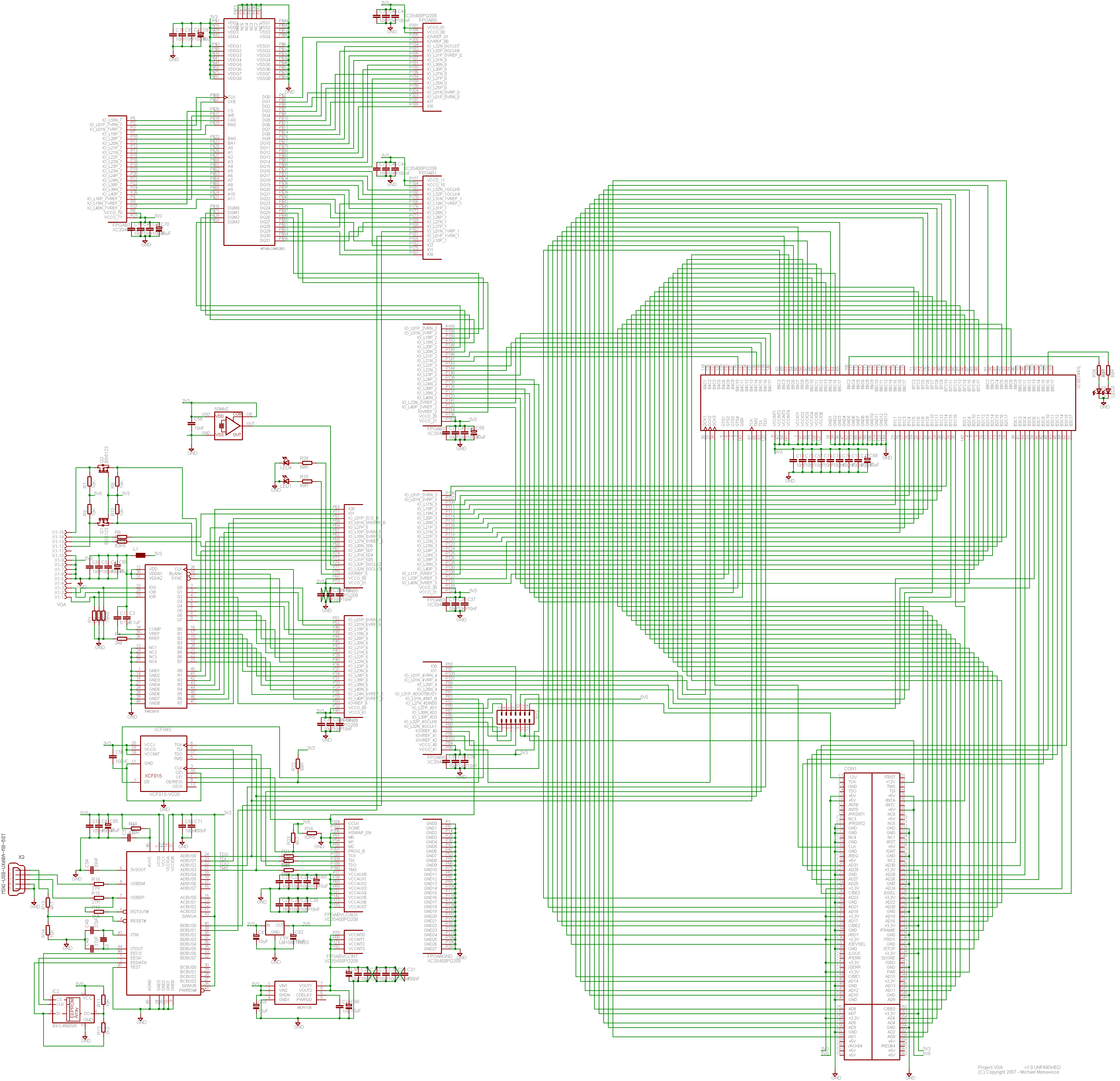
Updated schematic
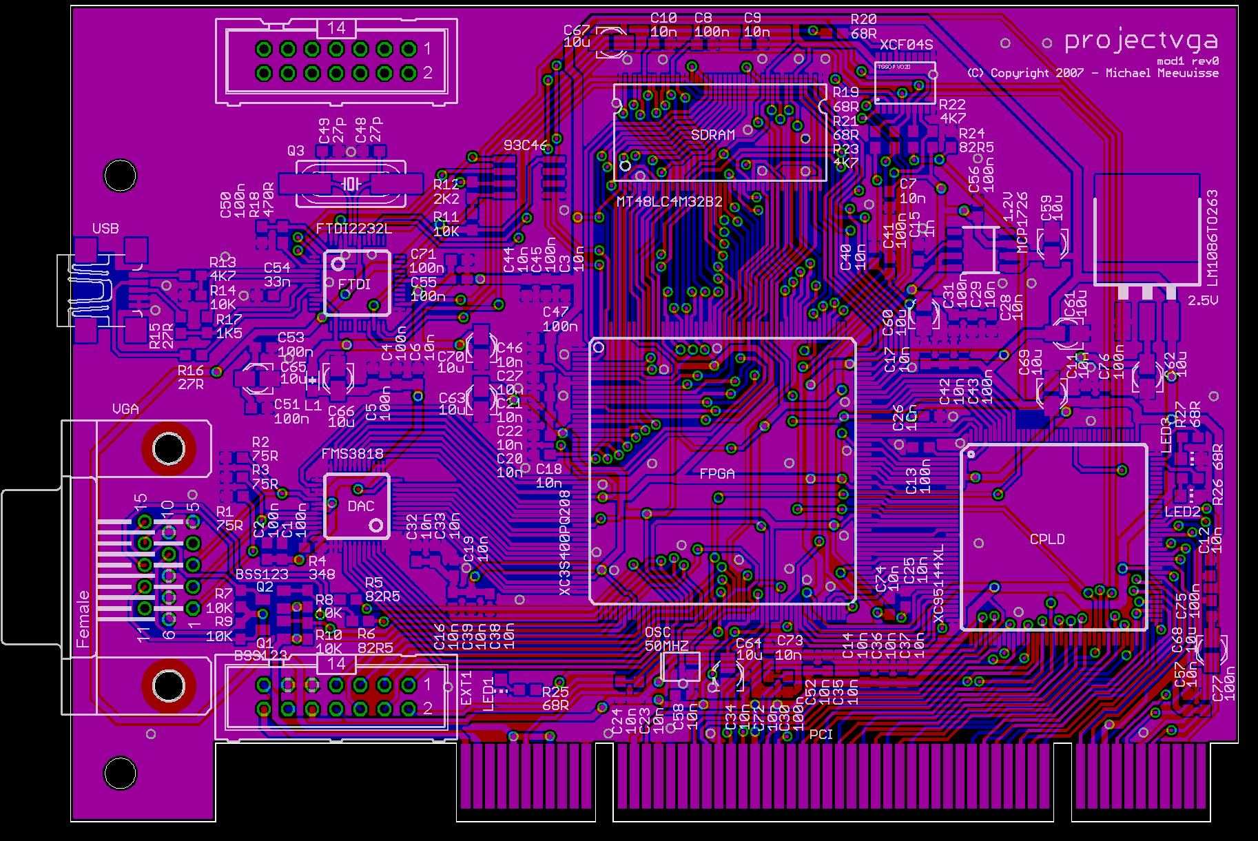
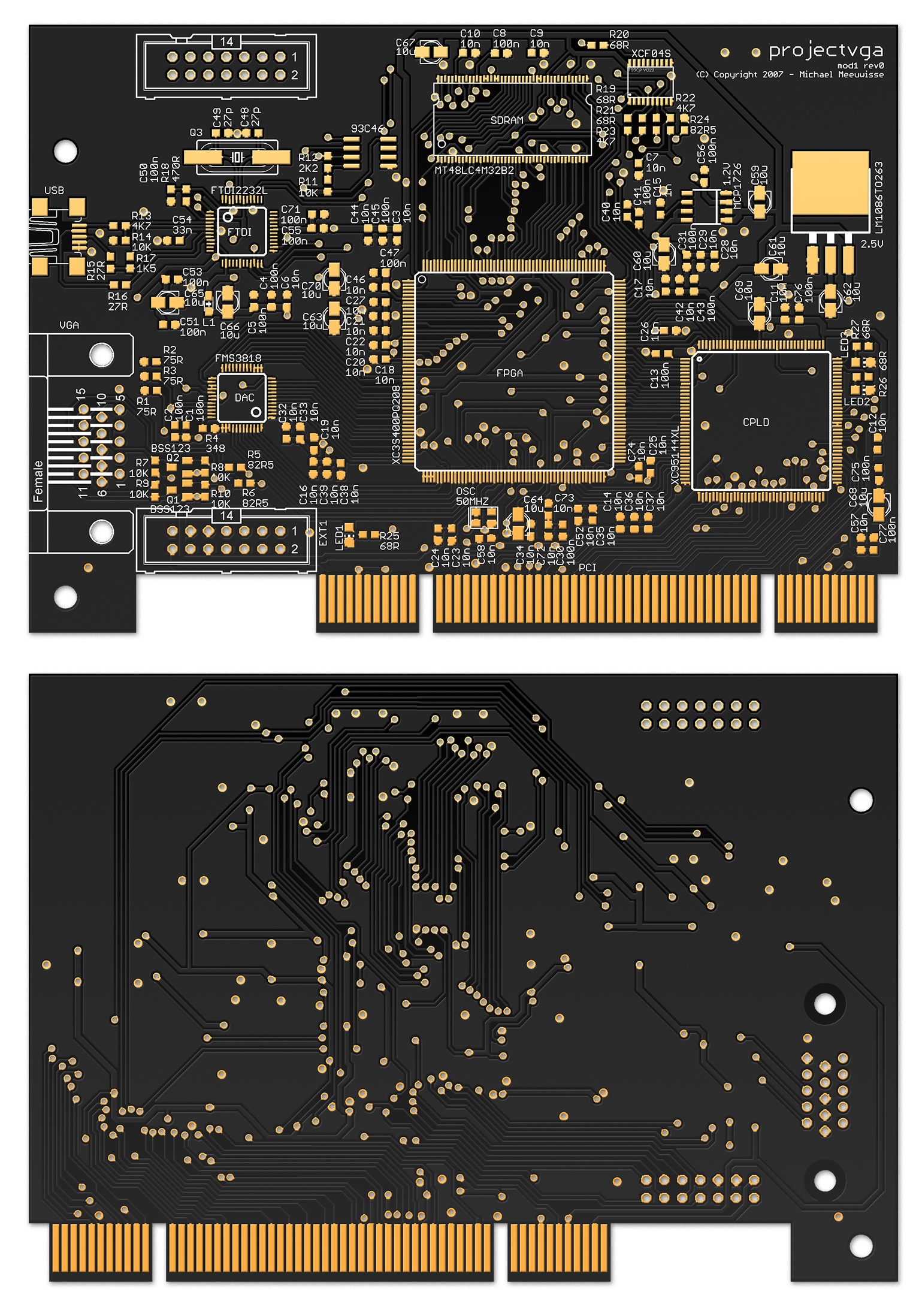
So anyway, communication. Quite a few points about the choice of components were already discussed in "Motivation #1" so I like to focus on the buses today. There are a few buses on the card of which most are fairly obvious and one is very roughly defined. While I'm at it I'll document which pins are used for what on the FPGA and CPLD. I've got it here on paper, but it's nicer to have it available online. The layout of the card is very straightforward so I didn't make an overview image. I'll leave that to your imagination. For all the exact pinouts of the chips, see their datasheets which I've listed here for your convenience. Be aware that they're all PDFs and could be a couple of Megabytes.
- PCI Specification 2.2 - Sorry, not going to give you that one due to copyright issues.
- FPGA: XC3S400 PQ208
- CPLD: XC95144XL TQ144
- SDRAM: MT48LC4M32B2
- DAC: FMS3818
- USB: FT2232D/L
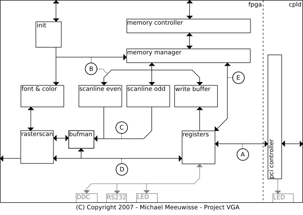
Block Diagram
A: PCI to CPLD
The card is designed to be 3.3V and 5V compatible and should be able to run on 33MHz and 66Mhz, although 66MHz
is very much dependend on how fast the CPLD can go with the code I'm going to write for it. Which means I don't
know yet if that'll work. Anyway, for 3.3V and 5V compatibility the CPLD needs to accept both voltage levels and
it does this out of the box as long as it's powered by a 3.3V supply. The clock is supplied by the PCI bus and
needs to be connected to a GCK pin on the CPLD. In this case, it ended up being GCK3 (pin 38). Then all the required
signals are connected to the right of this pin, except for INTA which I added at the last moment and is connected
to pin 35 of the CPLD. They are basically added in order, with the top and bottom side taking turns. That means
that RST is next on pin 39, AD31 on pin 40, etc. In order, you get; RST, AD[31:24], CBE3, IDSEL, AD[32:16], CBE2,
FRAME, IRDY, TRDY, DEVSEL, STOP, PAR, CBE1, AD[15:8], CBE0 and last but not least AD[7:0]. Naturally some dedicated
pins are in between but I left those out for clarity, if you count this out you end up with AD0 being pin 94. You
can see how this ends up in which function block / macrocell in the schematic, since I've made the eagle lib to
display that information. On the PCI connector only PRSNT2# is tied to ground, which configures the card as
consuming a maximum of 15 watt.
B: CPLD to FPGA
The other main connection of the CPLD is the databus to the FPGA. This databus is very broadly defined right now
because I simply don't know how much I'll be able to offload into the CPLD. The idea is that in the worst case
I can forward almost all signals to the FPGA, including the PCI clock. If, however, I'm going to do two clock
domains in the CPLD I've still got that option since GCK1 and GCK2 are connected to the FPGA. Also I don't know
if the GTS and GSR pins will be any use to me, so I made sure those are included. If I don't need them for their
special purpose I can always use them as general IO. The idea is that I have 6 'control' lines (including clock)
and 32 address/data lines. Not that I'll need them all as address (I can only access 16MB after all in the SDRAM)
so there might be some extra encoding there. In any case, how these pins will be used is somewhat unclear right
now and the only point of 38 lines is that it's pretty certain that this will be enough. The lines start above
the INTA line of the PCI connection and count all the way up until pin 135. I've declared the order to be C[0:2],
AD[31:0], C[3:5], but since GTS2,1,4,3,GSR is AD9,8,6,5,4 respectively this might change in the future. It's only
a naming convention anyway.
On the FPGA side of the story is most of bank 2, 3 and 4 dedicated to this connection. The SDRAM connection needed a few extra pins so the top of bank 2 is used for that, and bank 4 wasn't used entirely so the expansion connector sits there. But more about that one later. C5 is connected to IO_L21N_2, or pin 147, and everything else is a linear connection to the other side (skipping naturally the dedicated pins). A special note for pin 102 which is used for a clock to the EEPROM after configuration of the FPGA, and is skipped too for this connection. That makes the last pin, C0, end up on IO_L25P_4, or pin 94.
C: FPGA to SDRAM
The pinout of the SDRAM is somewhat odd in certain areas but I figured I could route them in such a way that it
makes mostly perfect sense for the FPGA. That's a contradiction, isn't it? In any case, the bus connects to bank
7, 0, 1 and a tiny bit of bank 2. The order of signals is the address lines A[11:0] starting at the bottom of bank
7, then all the control lines BA1, BA0 (which you could technically count as address lines, and probablly will be
used as such) followed by CS, RAS, CAS, WE, CKE, CLK. Here, the corner of the FPGA is reached so there's plenty
of room to get a good signal for CLK, and starting on bank 0 (pin 205) are the data lines DQ[0:15]. On bank 1 are
the lines DQ[16:28], and since the JTAG connection is at the end of this bank, two pins are used to create a
serial data connection to the B-bus of the USB controller. This can essentially be used as a 3.3V rs232
connection. However, due to these lines DQ[29:31] (not that they'd fit anyway on bank 1) are located at the
start of bank 2. Finally, DQM[0:3] are connected. These datamask lines will probably not be used, but might be
useful for something so are present anyway.
D: FPGA to DAC
The connection to the DAC is very simple since it's pinout makes a lot of sense. One side of the IC is dedicated
to the 'sensitive' signals and is directed to the VGA analog out. This side also contains the CLK signal which
therefore has to travel the furthest unfortunately. On the FPGA bank 5 and 6 are dedicated for this connection
so to make sure the CLK signal has enough routing space, this is connected at the top of bank 6 (pin 28). Right
after that the top of the DAC (it's upside down to get the analog side on the left) is connected. The order of
signals ends up being; CLK, B[7:0], SYNC, BLANK and G[7:0]. R[7:0] is located on bank 5 and after that the digital
VGA signal follow. HSYNC and VSYNC connect by means of a simple resistor, SDA and SCL go through a level shift
to get from the 3.3V FPGA IO at 5V DDC (an I2C bus) level. The last 3 pins of bank 5 are connected to the 50MHz
clock and two leds for whatever purpose. Can't hurt for debugging or general status indication.
E: USB to JTAG and JTAG chain
The JTAG chain is the order in which the JTAG compatible chips are connected. In our case, the data comes from the
A-bus of the FT2232, then goes to the FPGA PROM, followed by the FPGA and finally through the CPLD. The FPGA is
in there because JTAG has some other features than just in system programming which might come in handy. The
signal is 3.3V all the way, but because the FPGA wants to see 2.5V voltage levels there are some resistors added
to get that effect. I've copied this from figure 4 in xapp453.
The PROM comes before the FPGA because I wanted to copy figure 1 in xapp694
as much as possible, although it probably won't matter much anyway. All JTAG signals are dedicated signals on
the PROM, FPGA and CPLD so it shouldn't be a mystery where everything goes. On the FT2232 however I've copied the
pinout of this programmer (see the logical diagram) to make sure
that this would work. It's probably even possible to use their software if xilinx' tools turn out to be ineffective.
The PCI connector isn't in this chain because (rumor has it) a lot of consumer motherboards don't actually implement
these signals at all. If I'd take it up in the chain, I'd need some extra logic to detect this and only a few people
would be able to use it. Not worth the effort, thus left out.
F: FPGA to expansion connector
Right, after all these buses, I still had some pins left. The logic cells of the CPLD would be almost definately
be completely used up so the 80 or so data lines left there are a pity, but whatever. More interesting is that I've
got exactly 8 lines remaining at the bottom of the FPGA in bank 4. These lines (between pin 79 and 93) are
connected to an expansion connector for your entertainment. They're not buffered or anything, so don't hotplug
stuff on it or you might kill the FPGA. And they're 3.3V only! If you want to do anything with these pins, it's
your own responsibility. The full pinout of the connector (with pin 1 being top right, pin 2 bottom right, etc)
is as follows; pin 1 - 8 are data signals (see the schematic for exact names), pin 9 and 11 are ground, pin 10
is 3.3V, pin 12 is 5V, pin 13 is +12V and pin 14 is -12V. Be careful with these last two as they can only provide
little power; +12V max 500mA and -12V max 100mA.
Well, that's all for now. See ya later!
[: wacco :]